Space Charge: Definition, Examples, and Effects
What is Space Change in PN Junction
A space charge is defined as a region of space where electric charges accumulate, either in free space or in a dielectric material. Electric charges can be either positive or negative, and can be mobile or immobile. Space charge can affect the electric field, electric potential, and current flow in a region.
Space charge can occur in various situations such as
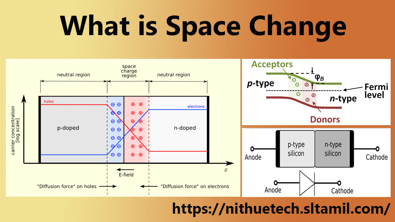
Semiconductor junctions: When a p-type semiconductor (which has excess holes) comes into contact with an n-type semiconductor (which has excess electrons), the electrons and holes near the junction recombine, leaving stationary ions behind. This creates a space charge region that is depleted of mobile charge carriers and has an electric field that prevents the charges from spreading further. This region is also called the depletion layer or the depletion zone.
Tubes: When a tube (such as a vacuum tube or thermionic converter) is energized, electrons are emitted from the cathode (negative electrode) and move toward the anode (positive electrode). However, the electrons take some time to pass through the tube and can form a cloud of negative charges near the cathode. This creates a space charge region that repels the emitted electrons and reduces current flow. This area is also called cathode fall or virtual cathode.
Dielectric breakdown: When a high voltage is applied to a dielectric material (such as a capacitor or power cable), electrical charges can be injected from the electrodes into the material or ionized in the material. These charges can become trapped in the material or move under the electric field. This creates a space charge region that distorts the electric field and increases the electric stress in the material. This can lead to dielectric breakdown, which is a breakdown of the insulating properties of the material.
Water Trees: Water trees are tree-like structures that form in water-impregnated polymer insulated cables. They are caused by partial discharges, which are small sparks that occur in the cable due to high voltage stress. The partial discharges create regions of space charge that attract water molecules and form branches of water-filled cavities. These branches weaken the insulation of the cable and reduce its life.
Effects of space charge
Space charge can have both positive and negative effects on various devices and applications, such as:
Thermionic converters: Thermionic converters are devices that convert heat into electricity using thermionic emission, which is the emission of electrons from a hot metal surface. Space charge reduces the efficiency and power output of thermionic converters by creating an additional barrier for emitted electrons. To overcome this barrier, higher temperatures or lower voltages are required, which increase heat loss or decrease the output voltage.
Amplifiers: Amplifiers are devices that increase the amplitude of an input signal using a tube or transistor. Space charge can improve the performance of amplifiers by creating a negative voltage across some of the tubes, which is equivalent to providing a negative bias. This distortion helps control the amplification process and reduce distortion.
Shot Noise: Shot noise is a type of noise produced by random fluctuations in electric current due to discrete charges. A space charge can reduce gunshot noise by affecting the movement of projectiles along their trajectory. This reduces the number of rounds that randomly arrive at a given point, thereby reducing their statistical variance, which is shot noise.
PN junction diode
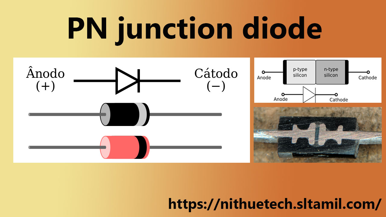
A PN junction diode is formed when a p-type semiconductor is fused to an n-type semiconductor, creating a potential barrier voltage across the diode junction.
A PN junction diode consists of a p-region and an n-region separated by depletion regions where charge is stored. The effect described in the previous tutorial is achieved without any external voltage being applied to the current PN junction, resulting in the junction being in an equilibrium state.
However, if we were to make electrical connections at the ends of both the N-type and P-type materials and then connect them to a battery source, there is now another source of energy to overcome the potential barrier.
The effect of adding this additional energy source is that the free electrons are able to cross the depletion region from one side to the other. The behavior of the PN junction with respect to the width of the potential barrier creates an asymmetrical conducting two terminal device, better known as a PN Junction Diode.
Two types of bipolar transistors
There are two types of junction transistors and they are:
- NPN transistor
- PNP transistor
In an n-p-n junction transistor, the p-type has the majority charge carriers and the other two ends have the n-type majority carriers. On the other hand, in the p-n-p transistor, the n-type has the minority charge carriers while the other two arms have the p-type majority carriers.
NPN transistor
In an NPN transistor, a p-type semiconductor base is inserted between an n-doped emitter and an n-doped collector. NPN transistors are the most widely used bipolar transistors because of the ease of electron mobility versus hole mobility.
The figure shows the construction and symbol of NPN transistors. The majority charge carriers in an n-p-n transistor are electrons and holes are the minority charge carriers. A small amount of current at the base terminal will cause a large amount of current to flow from the emitter to the collector. Due to the forward biasing of the transistor, most of the charge carriers in the emitter will bounce towards the base. Electron-hole recombination at the base is very small in the base region and most of the electrons pass to the collector region.
PNP transistor
In a PNP transistor, an n-type semiconductor base is inserted between a p-doped emitter and a p-doped collector. In this type of transistor, holes are the majority carriers and electrons are the minority carriers. In a PNP transistor, the emitter is forward biased and the collector is reverse biased.
Stay tuned to BYJU'S to learn more about diodes, semiconductor devices and many more through interesting video lectures.


